An overview of the BMC
In this post, we take a deeper dive into the BMC hardware and how it is connected to the Enzian’s mainboard.
As we discussed in our Booting Part 1 post, the BMC is a very important part of an Enzian board. It is responsible for powering, supervising and regulating the Enzian system. Its tasks include:
- Powering the Enzian system up and down
- Driving voltage regulators for CPU, FPGA, DRAM, clocks, fans, etc.
- Controlling fan speed
- Monitoring system health
- Emergency shutdowns
From a research perspective, it can also be used for all kinds of useful measurement applications.
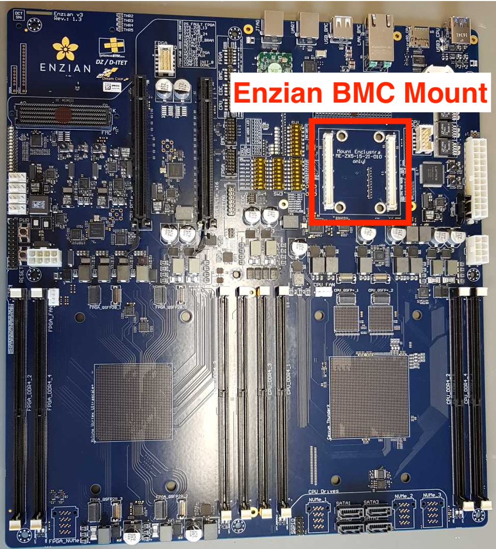
The BMC sits behind the IO shield, mounted on the Enzian mainboard via two pin banks.
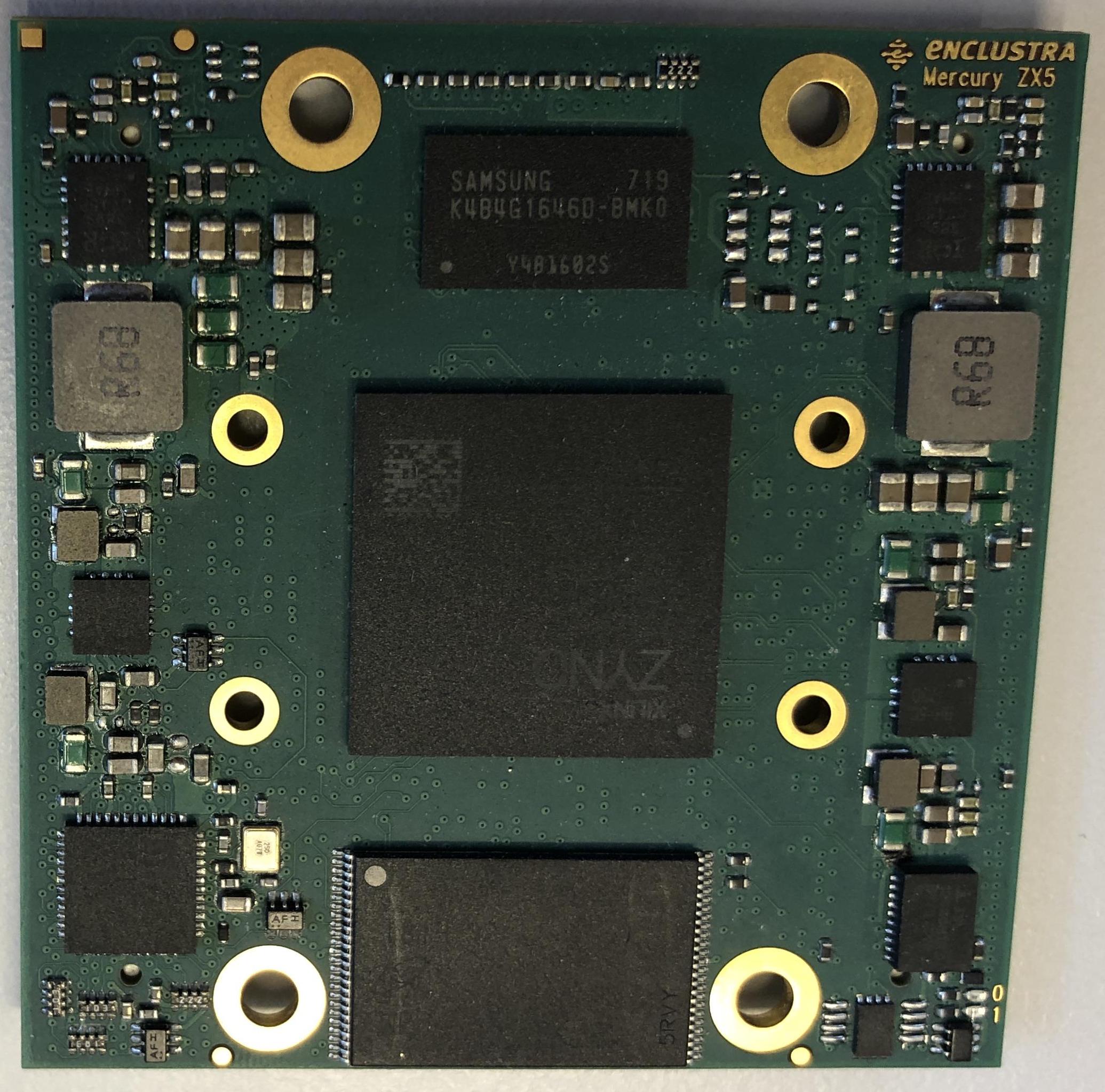
The current BMC used on the Enzian boards is an Enclustra Mercury ZX5 module, based on a Xilinx Zynq 7000 SoC.
Xilinx Zynq 7000 SoC
The Zynq 7000 SoC has two Cortex A9 cores on a 28nm Xilinx FPGA, completely separate from the main Enzian FPGA. Giving the BMC its own FPGA is overkill for a cost-optimized, mass-produced mainboard which already went through various test revisions. However, for a university research group which dabbles in hardware design, it gives us the flexibility to correct oversights and mistakes on the Enzian board.
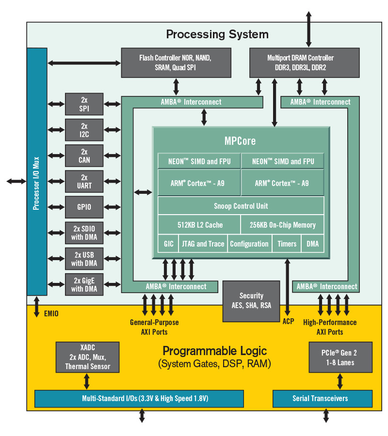
For example, we noticed missing pull-up resistors on some I²C lines on the current version of the Enzian mainboard: instead having to run an expensive redesign and fabrication run of yet another Enzian mainboard, we were able to update the FPGA bitstream on the BMC side, saving us money, time and nerves. Moreover, the BMC’s FPGA allows us to research if and how offloading complex operations to custom circuitry can help us build safer or more efficient BMCs.
Enclustra Mercury ZX5
The Enclustra Mercury ZX5 board adds useful bits and bobs to the central Zynq 7000 SoC, such as:
- 1GB DDR3 RAM
- 512MB of NAND flash
- 64MB of quad SPI (NOR) flash
- a PCIe 2.0 x4 slot
- 1 Gbit Ethernet
- 178 user I/O pins
- 146 are connected to the FPGA
- 12 are ARM peripheral I/Os
- 20 are MGTs (short for Multi-Gigabit Transcievers)

Some of the BMC’s connections are routed to the Enzian’s rear panel, such as the Ethernet port, and a USB port, shown here:
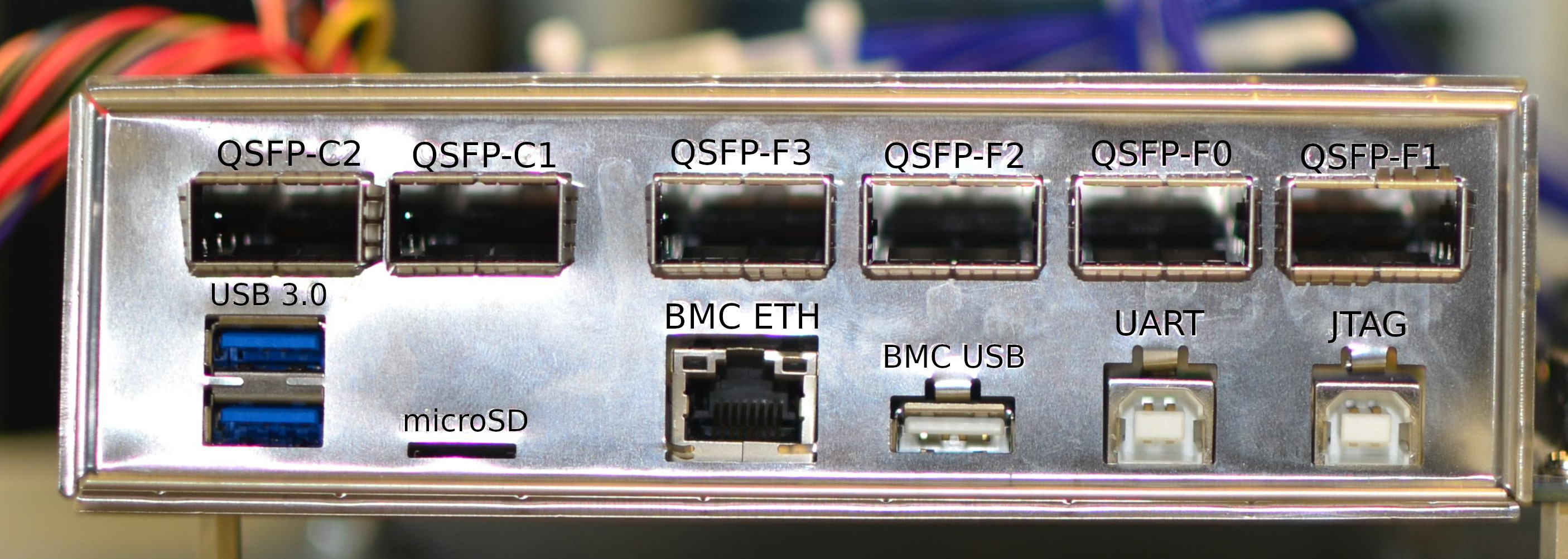
Most of the I/O pins are wired to the BMC’s FPGA, such as the clock, data and alert lines of the many Enzian I²C buses. These buses connect clock generators, voltage regulators and current sensors that the BMC interacts with to drive an Enzian system. From the FPGA fabric, we can then either integrate these connections in custom driver ciruitry or pass them through to Linux on the BMC to control them from software.
Not all the BMC’s IO pins are connected to the Enzian mainboard. Since we made the Enzian schematics openly available, the full set of connections can be found there.
Technical limitations
Even considering the flexibility of our overpowered BMC, a couple of design decisions were sub-optimal in retrospect:
- The BMC’s UART (serial console port) is routed through the FPGA, which makes debugging first-level boot loader issues tedious (although not impossible).
- The Cortex-A9 cores do not support hardware-accelerated virtualization, since they do not support the ARMv7 hypervisor mode.
These limitations are not essential for basic system operation, and we are already successfully using the Mercury ZX5 boards in practice to drive our 9 fully functional Enzians.
A new BMC board for further research opportunities
However, we are especially interested in having hardware-accelerated virtualization on our BMCs to research and implement high-assurance BMC software stacks. Having successfully booted seL4 on the ZX5 board, we want to utilize seL4’s virtualization support to look further into building secure board management controllers.
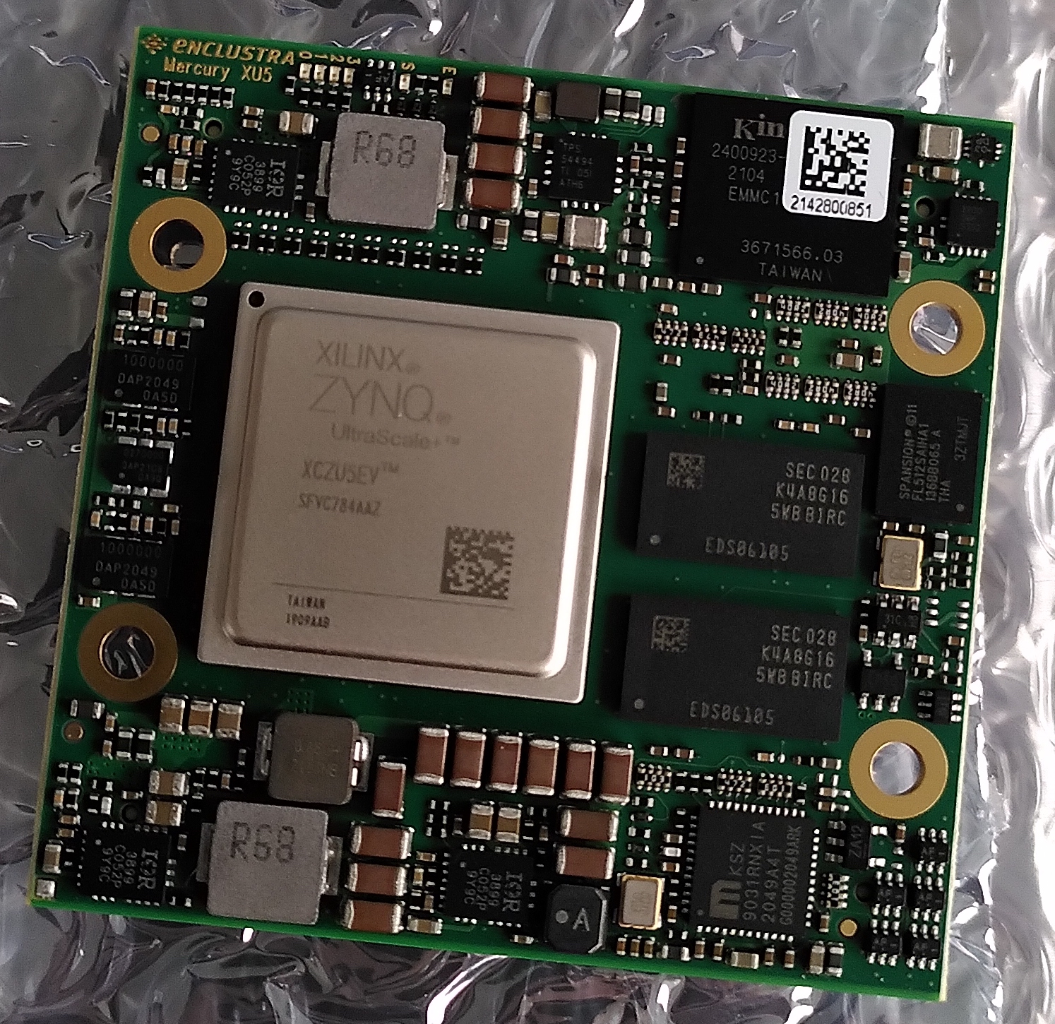
As a result, we ordered an even more over-the-top board, the Enclustra Mercury XU5. It is based on the Xilinx Zynq UltraScale+ MPSoCs, which include two Cortex-A53 cores and a 16nm Virtex UltraScale+ FPGA. The CPU cores support the ARMv8 architecture, which allows us to run hardware-accelerated virtualized workloads on top of seL4.
The Mercury XU5 board comes with 4GB of ECC DDR4 RAM on the CPU side and 1GB of DDR4 RAM on the FPGA side. Unfortunately, it is not quite pin-compatible with the ZX5 board we currently use, and so we will have to design a small shim board to scale voltages between the connections on the Enzian mainboard and the new XU5. However, we can also solve the BMC’s UART routing problem in the shim board, by swapping pin connections around so that the BMC’s UART is directly connected to the corresponding lines on the Enzian board.
