Subscribe to the mailing list for updates.
April 16, 2020
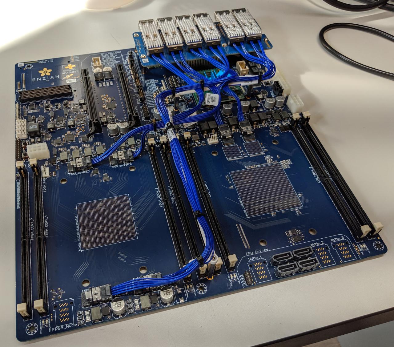
Assembled Enzian v.1.3 board
When we got the first boards back late last year, they were not functional - in particular, an error in the design made it impossible to power up the FPGA or CPU. This was caught by the company doing the assembly, so we didn’t have the two big chips soldered on.
However, Dream Chip were able to test all the low-speed signals on the rest of the board, which all seemed to work, so we could actually use the board to help develop the firmware for the Board Management Controller (BMC).
We also decided to take the opportunity to do high-speed signal integrity testing on the board: even though the revised board would be slightly different, we might still flag problems early. And it sounded like fun…
Here’s the assembled board that Dream Chip sent to us for testing. You can see the SATA connectors for the CPU, and the spaces for the NVMe connectors on both sides. One of the board errors was that these should have had holes…
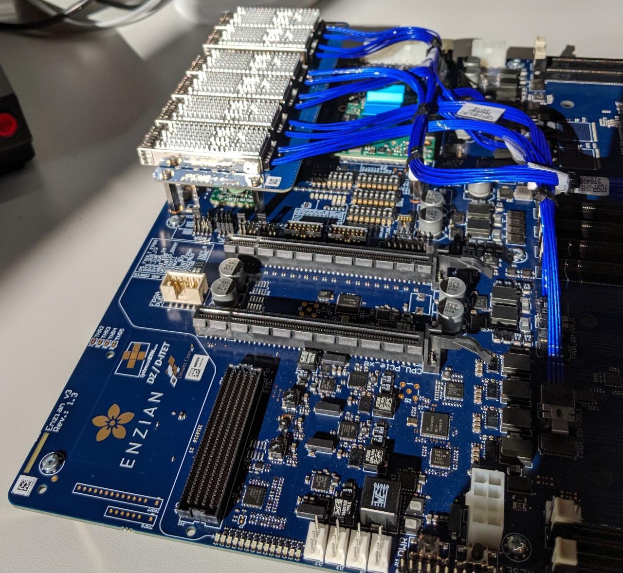
Here’s another view of the rear half of the board showing the two PCIe connectors (one for each side of the system), and the FMC connector for the FPGA:
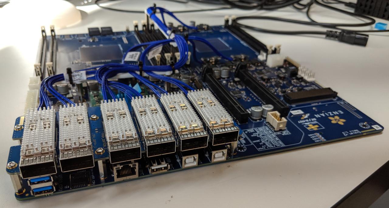
And, finally, this is the rear of the board, with the 6 QSFP28 cages (two for the ThunderX, 4 for the FPGA), plus USB3, and connectors for the BMC - USB connectors for the UARTs, and the Ethernet management interface.